


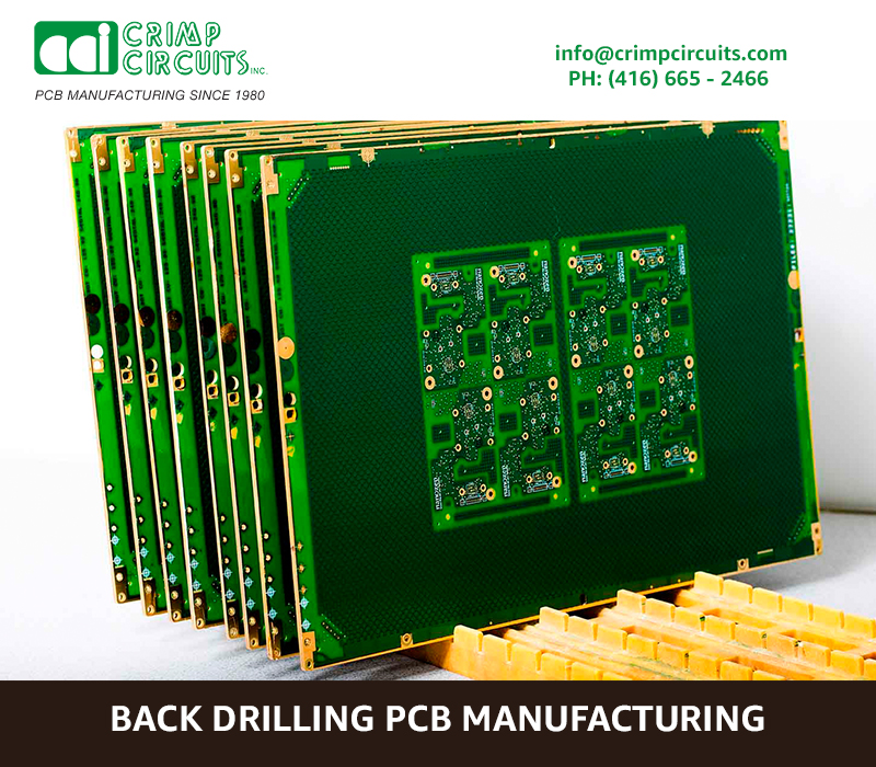
Brief about Back Drilling PCB Manufacturing
What is Back Drilling PCB Manufacturing?
Back drilling PCB manufacturing technology is basically used in semiconductor industry that ensures the highest fidelity signals can be carried at every increasing speeds. For this it should be ensured that the signal stubs are minimized. Now the question that arises here is what are stubs? So stubs are the source of impedance discontinuities and signals reflections which become more critical as data rates increase. Basically this is the preferred method in HS designs. Electrically they connect two or more layers together and serve as a convenient connecting point for traces and components throughout a multilayer PCB.
The general characteristics of Back Drilling PCB manufacturing
The basic and general characteristics of Back Drilling PCB manufacturing are mentioned below:
- It mostly contains rigid boards on the back.
- It is usually used on 8 or above layers.
- Its board thickness is over 2.5mm
- And minimum hold size is 0.3mm

What are the advantages of back drilling PCB?
The advantages of using back drilling PCB manufacturing have been mentioned below:
- It reduces the deterministic jitters
- It also lowers the bit error rate or the BER
- It encourages less signal attenuation with improved impedance matching
- Increases the data rates
- Increases channel bandwidth
- Reduces EMI/EMC radiation from the stub end
- Reduces the excitation of resonance modes
- Also reduces the via-to-via cross-talk
- It also lowers the cost than the sequential lamination
What is the process of Back drill?
The main process of Back drill is mentioned below in steps:
- Providing PCB with tooling whole, and make drilling process.
- After this, plate the hole before dry film sealing treatment.
- Make outer graphics after the plating process.
- After that the process of performing patter plating on the PCB takes place after forming outer pattern, and also performing dry film sealing treatment of the positioning hole before pattern plating.
- Then you need to drill the tooling hole and then drill back vias on need.
- At last remove the residual after drilling back vias and cleaning them.